2D/3D perovskite bilayer heterostructures hold potential for improving the performance and durability of various electronic and photonic devices, including photovoltaics, light-emitting diodes, photodetectors, lasers, and transistors. However, maintaining this performance depends on the stability of the cell’s 2D interlayer.
Recently, researchers from the Massachusetts Institute of Technology (MIT), the Samsung Advanced Institute for Nanotechnology at Sungkyunkwan University (SAINT), the National Renewable Energy Laboratory (NREL), Marmara University, and Lawrence Berkeley National Laboratory optimized the thin-film deposition of 2D perovskites using a hybrid solvent approach to achieve phase purity and high crystallinity.
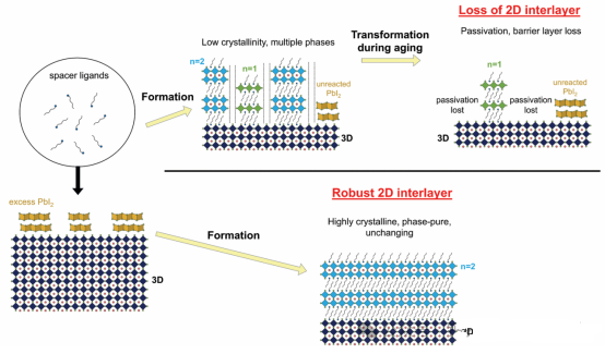
In this 2D/3D structure, the 2D interlayer consists of one or multiple stacked layers of organic-inorganic hybrid perovskites. The 2D interlayer protects the 3D perovskite in the stack by reducing the negative effects of material defects, controlling the movement of electrons or ions within the material, generating built-in potentials, preventing ions or electrons from migrating from the environment into the material, and inhibiting ion migration. This interlayer enhances both the photoelectric conversion efficiency and stability of the device. As the device ages, the 2D interlayer evolves in different ways, thereby altering the device’s stability.


