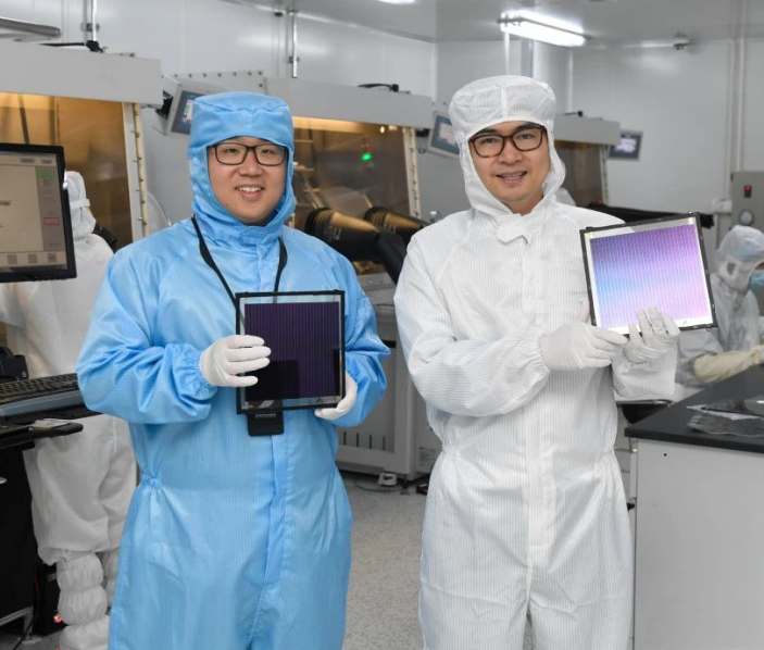
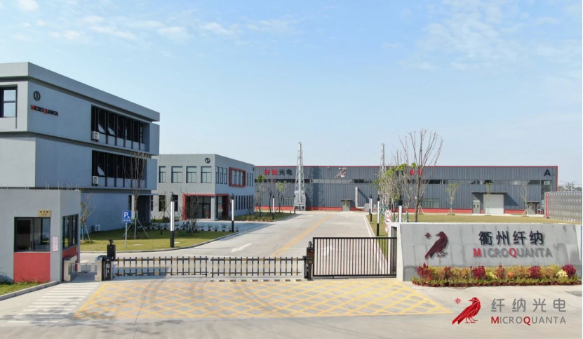
In 2015, Dr. Yao Jizhong and Dr. Yan Buyi, both returnees from overseas studies, co-founded Microquanta Semiconductor, establishing roots in the perovskite photovoltaic sector. Over the past decade, the Hangzhou-based firm has emerged as a global pioneer in perovskite technology, specializing in cutting-edge R&D, low-carbon manufacturing, and commercial deployment of perovskite modules. By 2024, it accounted for 52.2% of the global perovskite module shipments.
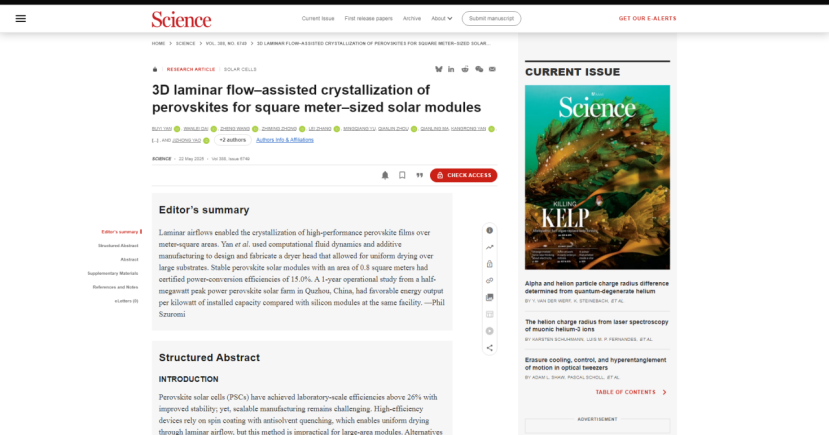
On May 22, Hangzhou Microquanta Semiconductor Co., Ltd., as the primary corresponding author, published a research paper titled “3D Laminar Flow-Assisted Crystallization of Perovskites for Square Meter-Sized Solar Modules” in Science, a top-tier international academic journal. The study systematically outlined an industrialization pathway for achieving balanced efficiency, stability, and manufacturing yield in square-meter-scale perovskite modules—a first for a Chinese enterprise publishing independently as the primary author in Science.
The research team, led by Microquanta, pioneered the 3D Laminar Flow-Assisted Drying (LAD) technology with full independent intellectual property rights. By integrating theoretical calculations with 3D printing, the method constructs a large-area, uniform airflow field. “This approach strategically combines the aerodynamic advantages of conventional spin-coating and vacuum flash evaporation processes while mitigating their respective drawbacks in large-scale production and stability,” noted Yan Buyi, co-founder and CTO of Microquanta. Backed by policy support from science and technology departments and collaborative efforts with Zhejiang University and Zhejiang Sci-Tech University in efficiency optimization and theoretical modeling, the innovation resolved the industry-wide challenge of balancing efficiency and stability in large-area perovskite modules, significantly improving production yields.
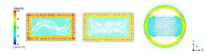
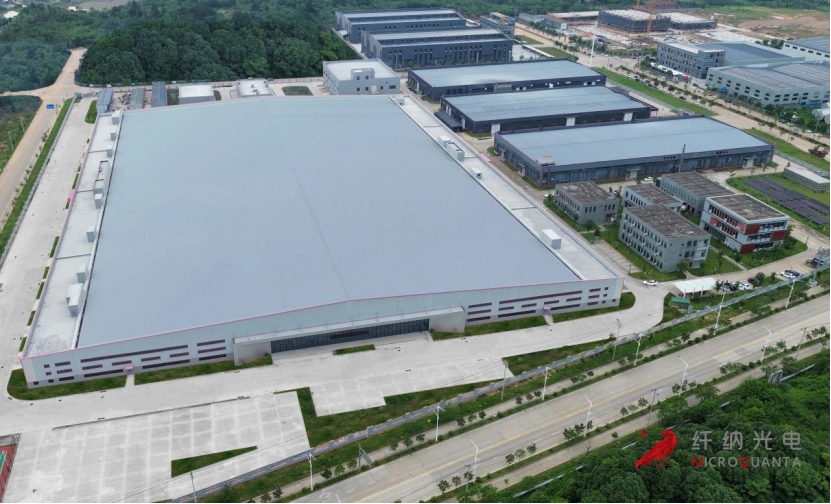
“Compared to traditional vacuum flash evaporation, LAD technology overcomes uncontrollable crystallization processes, reducing residual solvents in thin films by 90%. This minimizes surface defects, optimizes crystal morphology, and fundamentally addresses low manufacturing yields while enhancing photothermal stability,” Yan explained. Leveraging this technology, Microquanta established the world’s first 100-MW perovskite production line, setting multiple global records in the perovskite sector. The line achieved a manufacturing yield exceeding 98.5%, reaching commercialization standards.
“This breakthrough reshapes the trajectory of perovskite photovoltaics. By deploying LAD technology, Microquanta has accelerated perovskite commercialization, completing the world’s first megawatt-scale perovskite distributed rooftop power plant and ground-mounted power station, both connected to the grid,” stated Yao Jizhong, co-founder and CEO of Microquanta.
To date, Microquanta’s proprietary technologies have yielded over 300 global patents (80% invention patents), with core patents authorized in China, the U.S., Europe, and Japan, fortifying its full-industry-chain competitive edge in equipment, processes, and materials.


