A research team of University of Science and Technology of China recently has brought up a new structure solution for the long existed “passivation-transmission” contradiction problem of perovskite solar cells.
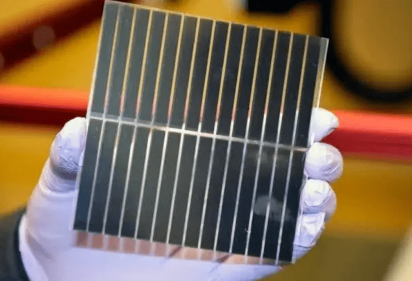
The breakthrough was achieved by the team led by Profess Xu Jixian and their partners. They named the solution Porous Insulator Contact (PIC) after rigorous model simulation and experiments. They also demonstrated the design principle and concept verification of PIC, which set world record on steady-state certification efficiency of p-i-n trans-structure devices. They were also applicable in multiple substrates and perovskite components.
Xu Jixian, a professor at the University of Science and Technology of China, and his collaborators proposed a new structure and breakthrough scheme named PIC (porous insulator contact), aiming at the “passivation transmission” contradiction problem that has been prevalent in perovskite solar cells for a long time. Based on , the design principle and concept verification of PIC scheme were given, and the world record of steady-state certification efficiency of p-i-n trans-structure devices was achieved, It also shows general applicability in a variety of substrates and perovskite components.
Relevant research results were published in the article “Reducing non-radiative recombination in perovskite solar cells with a porous insulator contact” on Science magazine on February 17.
The main idea of this study is not to rely on the traditional nanoscale passivation layer and tunneling transmission, but to directly use the porous insulation layer with the thickness of 100 nanometers, forcing the carrier to transmit through the local open hole area, while reducing the contact area.
The research team’s semiconductor device modeling and calculation revealed the key design principle that the PIC structure period should match the perovskite carrier transmission length. The PIC scheme is similar to the local contact technology in crystalline silicon solar cells. However, the difference is that the carrier diffusion length in perovskite is much shorter than that in monocrystalline silicon, which is greatly reduced from millimeter level to micrometer or even shorter.
This requires that the size and structure cycle of PIC should be at the level of 100 nanometers. The traditional local contact process of crystalline silicon can not directly meet this precision requirement, and the use of high-precision micro-nano processing technology is not fully developed in the preparation area and cost.
Towards this, researchers skillfully used the size effect of the nano-sheet to realize the preparation of this nanostructure by PIC growth mode from conventional Stranski-Krastanov mode to the Volmer-Weber mode.
The PIC scheme was verified in the p-i-n trans-structure widely used in multiplayer devices. The hole interface recombination speed was reduced from~60cm/s to 10cm/s and the single-junction maximum efficiency of 25.5% was achieved for the first time (the steady-state verification efficiency of p-i-n structure was 24.7%).


